How did the chip in my laptop get made?
A few months ago, I purchased a new laptop. The computational backbone within this laptop is Apple’s new “M1 Chip.” In this blog post, I’ll be providing an overview of how Apple’s chip design became an actual semiconductor chip in my laptop, via the wafer fabrication process.
Given the complexity of this process (one could argue it’s the world’s most complex design and manufacturing process!), and that these manufacturing processes are regularly changing and improving each year, this overview is likely mistaken in various subtle ways, so I encourage you to read through the references and do your own research if you’d like a more detailed understanding. In the future, I may also write a blog post focused on the chip design stage.
A die shot of Apple’s M1 Chip
Manufacturing this chip required vast global coordination, intricate supply chains, unbelievable technological innovation, and a decades-long commitment to the continuation of “Moore’s law” by semiconductor chip designers and fabricators.
I’m fascinated by the feats of human ingenuity that led to this, and I hope reading this post leaves you with a taste of this magic. I encourage you to watch the videos that are provided and to look at the diagrams and photos, as they should aid your understanding of what’s going on. Some of the videos are also spectacular (you’ll know it when you see it!).
The following short videos are nice introductions to this topic, that will help you orient towards the rest of this piece.
From sand to wafers
Sand is the building block for the vast majority of computer chips available today. High-purity quartz, a chemical compound of Silicon dioxide, is mined in places like the Spruce Pine Mining District in North Carolina (USA) by companies such as Sibelco (Belgium) and The Quartz Corp (Norway). The refining process includes washing the quartz with chemicals and air (called “flotation”) to remove impurities such as feldspar; magnetic separation to remove ferrous contaminants; acid leaching to dissolve other impurity minerals; and thermal processing (calcination) to remove residual organic compounds. The purity of the quartz for semiconductor manufacturing has to be >99.999%, which costs around $5,000-10,000 per tonne to mine and refine. The crucibles which house the silicon metal during the next phase of production have to be made of the purest form of quartz to avoid any defects and chemical reactions, and quartz of the requisite purity for these crucibles is primarily found in the Spruce Pine Mining District.
A quartz quarry in the Spruce Pine Mining District
High purity quartz being collected
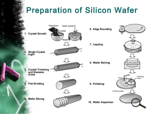
High-purity quartz is usually then exported to Japan, to be processed into silicon wafers by companies such as ShinEtsu and SUMCO (both Japanese), ready for chip fabrication. These companies take the quartz and reduce it to silicon metal, which is then processed further into an atomically perfect silicon ingot, via the Czochralski method.
Silicon wafers are produced by slicing these ingots, polishing them to ensure they are (very) flat, before a final inspection and sale to a semiconductor fabrication plant (aka “chip fab”, “fab” or “foundry”).
Building integrated circuits on a wafer
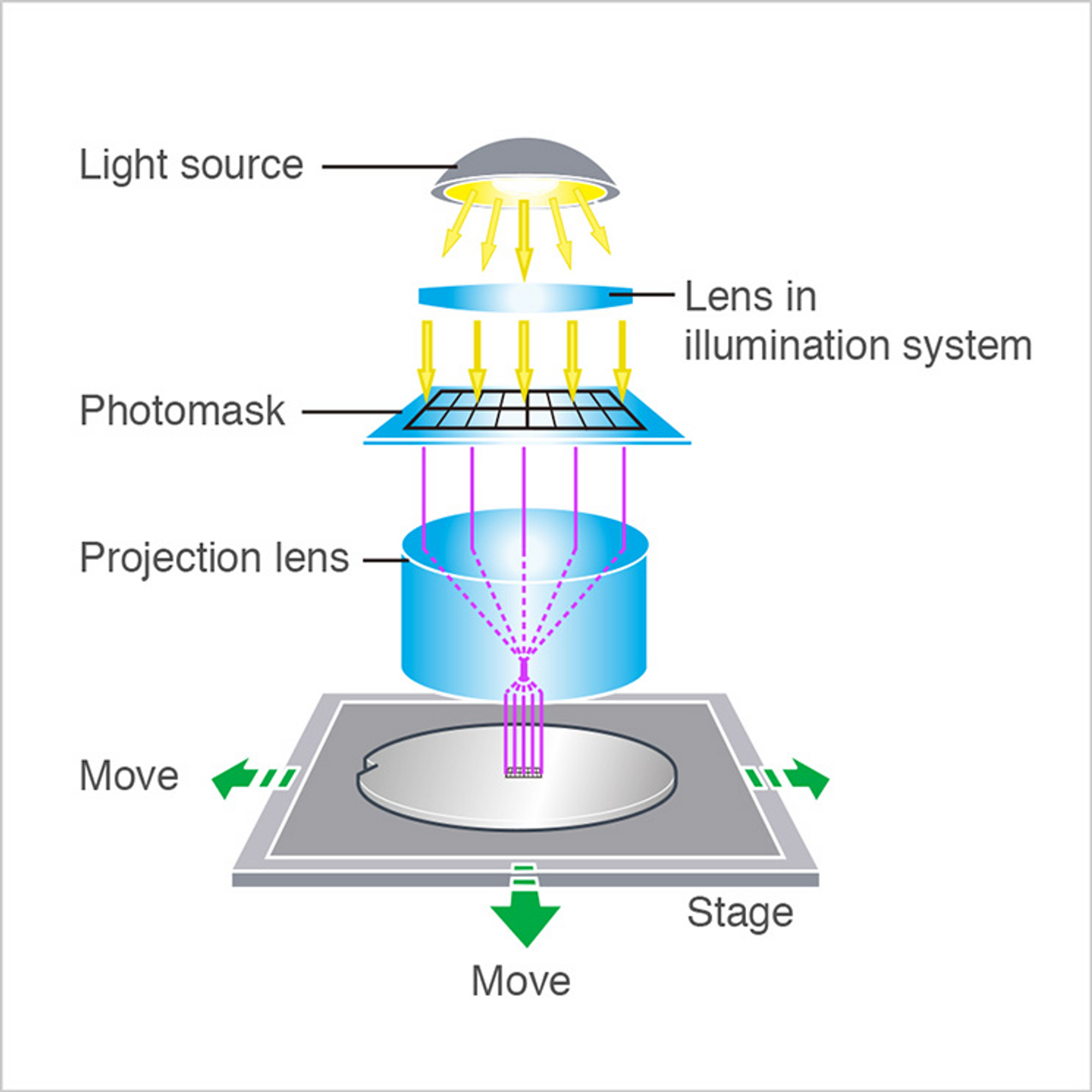
A silicon wafer by itself doesn’t have much value. In order to have commercial applications in the electronics industry, fabs “build” integrated circuits by “printing” billions of transistors and electrical connections on the wafer surface. This is done by carefully depositing thin films of materials onto the wafer, and using UV light to create specific (nano-meter scale) patterns in those materials. The patterns are determined by the chip designers, and those designs must be converted into photomasks that block certain parts of the wafer from being exposed to UV light, in order to create the patterns. This process of using light to produce patterned films of materials on a silicon wafer is called photolithography, and is explained in more detail below.
The company responsible for turning silicon wafers and other materials into Apple M1 chips is the Taiwanese Semiconductor Manufacturing Company (TSMC). TSMC is one of the world’s leading semiconductor manufacturing companies, fabricating a significant fraction of the world’s most advanced chips. The fabrication plant for the Apple M1 chip is TSMC’s leading fabrication plant, Fab 18. It’s located in Taiwan, and is estimated to have cost around $20 billion dollars to build.
Wafer preparation
Before a wafer is ready for the “printing” stage, they must test and prepare the surface for later processing. They inspect the wafer for defects, subject it to a thorough cleaning process, polish the wafer to the appropriate level of smoothness, and confirm the wafer is the correct thickness. Finally, to provide an interface between the wafer substrate and the layers that are printed on during later stages, they grow a small layer of silicon dioxide on the surface by heating the wafer in a furance.
Deposition
To form the desired layers and structures in an integrated circuit, thin films of materials such as metals, insulators and semiconductors are deposited onto the wafer surface. Metals like copper or alumnium are deposited to form interconnects, which act as wiring to electrically connect different components. Semiconductor materials such as silicon, germanium or gallium arsenide are used to create the transistors, which allow the amplification or switching of electrical signals within the chip. Insulating materials such as silicon dioxide are used to insulate different components from each other, to prevent electrical leakage.
Chemical vapor deposition is a common deposition technique, whereby the wafer surface is exposed to an easily vaporised starting material, which then reacts with or decomposes onto the surface. This process is conducted under high vacuum. Patterns are then etched into these materials via the lithography process described below.
Photoresist
Photoresists are materials that change characteristics when exposed to various wavelengths of light. They’re used by fabs to create the 3D patterns on the wafer surface, by coating the photoresist onto the wafer surface and exposing only certain parts of the photoresist to UV light. Once the photoresist has been applied via a spinning process, the wafer is “soft baked” to solidify the photoresist (and evoprate any remaining solvents, from previous photoresist applications). Most fabs apply a “positive” photoresist coating, which deteroriate when exposed to UV light, and can then be removed with a solvent to leave the desired pattern on the wafer surface.
Photomask
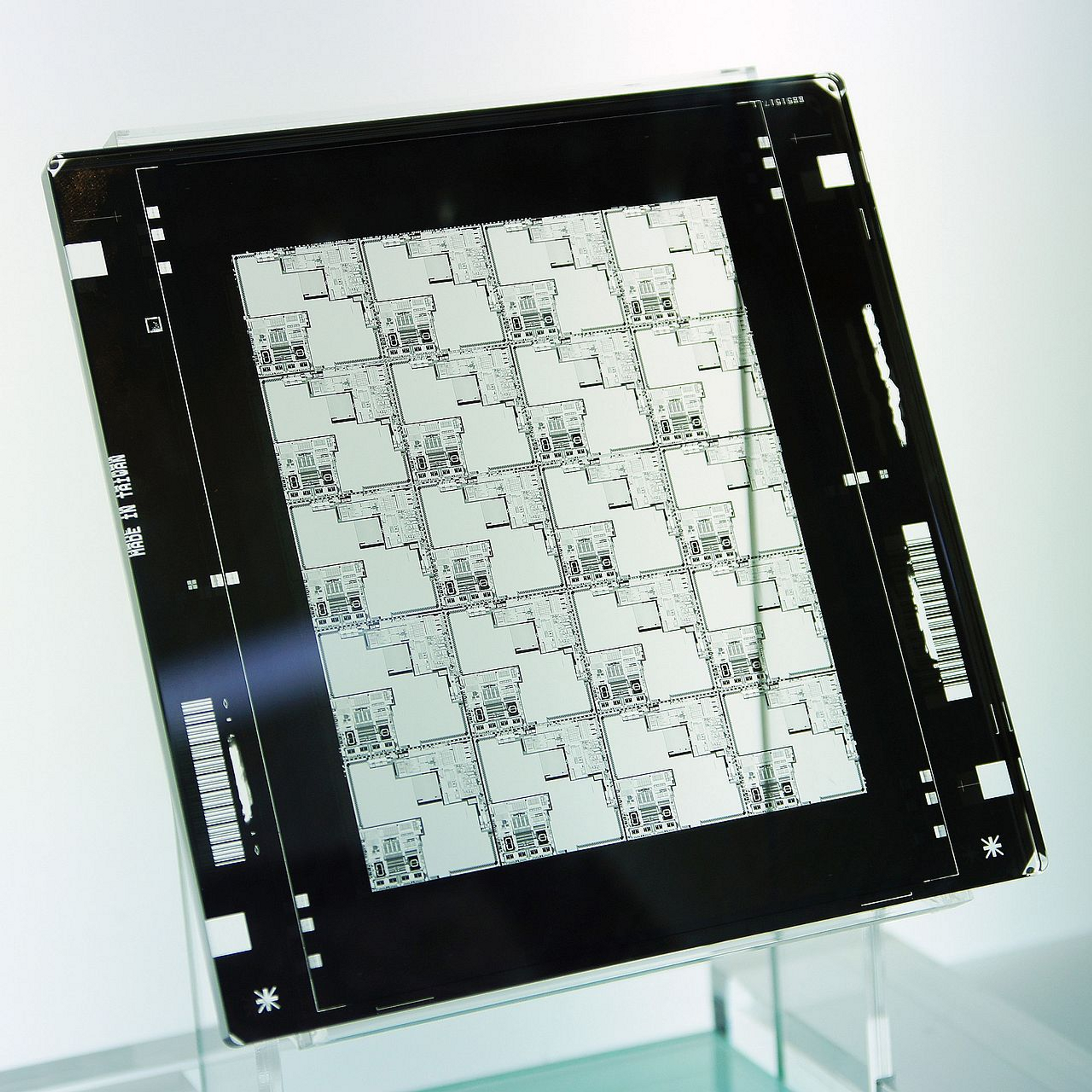
Once the chip designers have sent their designs to the fab, those designs are converted into photomask (or photoreticles), hereafter “masks.” Masks are the “blueprint” of an integrated circuit design, as they determine what patterns and circuits are developed on the silicon wafer. They’re usually made of highly transparent quartz glass, with a chrome stencil that prevents certain parts of the wafer from being exposed to UV light.
To print the same pattern across the wafer, the wafer is “stepped” from position to position until the entire wafer has been exposed to UV light through the mask. A single chip design may require a set of 10+ different masks to provide the instructions for the entire printing process, and the production of the blank photomasks is also a significant technical challenge due to the transparency required. Zeiss (Germany) is one of the leading manufacturers of blank photomasks.
Photolithography and EUV
Very low wavelengths of light are required to create the intricate features required for cutting-edge chips. An analogy here is that an artist needs a very fine pencil to draw intricate features in their artwork, and similarly, fabs require very small wavelengths of light to “draw” or print intricate features on the silicon wafer to create functional transistors. As a result, the wavelengths of light used during lithography have been trending downwards: in the 1970s and 1980s, visible light (400-700mm) was used, and by the 2000s, most semiconductor manufacturing used Deep Ultraviolet light (193nm). As of the early 2020s, the frontier is Extreme Ultraviolet (EUV) light, which has a wavelength of only 13.5nm.
To generate EUV light, one cannot use a regular bulb. Reliably creating EUV light is an immense technical challenge, which has been in the works since at least 1984, but it wasn’t until multiple breakthroughs at AMSL (Netherlands) in 2018 that it became commercially viable, through their new EUV lithography systems. TSMC purchase EUV lithography machines from ASML for a staggering price of $150M per machine.
Vaporising tin with lasers
ASML’s EUV machines use CO2 lasers produced by TRUMPF to create ultra-high powered 40kW laser pulses, easily strong enough to cut through steel. Molten droplets of tin of around 25 microns in diameter are then dropped into a vacuum chamber, where they’re initially hit by a low-intensity laser pulse to turn them into pancake-shaped plasma, followed by a “full-power” laser pulse which heats them up to 220,000 degrees Celsius and vaporises them, emitting EUV light. 50,000 droplets of tin are released into the vacuum chamber each second.
World’s best mirrors
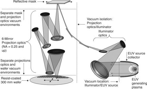
EUV light is absorbed by almost all materials, including air, so the EUV light column emitted by the vaporised tin must remain in high vacuum. Lenses cannot be used as they would also absorb the EUV light, so several mirrors are used to guide the EUV light through the mask and to the wafer, where the mask’s pattern is magnified by a factor of four.
Zeiss produces these mirrors (and the overall optics system), and these mirrors are the flattest objects humanity has ever created. If they were the size of Germany, the tallest mountain would be just 1mm high. They’re produced by depositing around 100 (nanometer-thin) layers of Molybdenum and silicon on top of each other. Mirrors composed of multiple thin films of dielectric material are also known as dielectric or Bragg mirrors. Precisely targeting this light onto the silicon wafer is also an immense technical challenge, requiring sensors that have nano-meter scale precision. Zeiss boasts that due to their mirror’s tilt stability, "if one of these EUV mirrors were to redirect a laser beam and aim it at the Moon, it would be able to hit a ping pong ball on the Moon’s surface.”
Hard bake and development
Once the photolithography stage is complete, the wafer is immersed in a developer solution to dissolve the exposed photoresist. The unexposed photoresist remains on the surface at this stage, in a pattern corresponding to the blueprint in the photomask.
The wafer is also “hard-baked” to harden the unexposed photoresist, to be resistant to subsequent processes (etching, deposition and ion implantation), before being removed entirely later.
Demonstration of Etching
Pattern transfer
To transfer the pattern into the substrate (or a thin film deposited above the substrate), pattern transfer techniques are used. The most commonly used pattern transfer approach is etching, which involves using gases (dry etching) or chemicals (wet etching) to selectively remove material from a thin layer on the surface of the substrate. The remaining photoresist “resists” the etching process, protecting the underlying material, whereas the unexposed substrate or film is “etched away”, leaving the desired pattern in the underlying layer.
Deposition is another pattern transfer technique. One deposition technique is atomic layer deposition (ALD) aim to deposit lay-ers of individual atoms onto the wafer surface. Meanwhile, selective deposition techniques (such as “Area-selective ALD”) aim to deposit layers of atoms in exact places on the surface, as opposed to covering the entire exposed surface. Deposition at this stage of the manufacturing process is often done to place copper interconnects onto the chip.
Finally, ion implamantation is a way to change the conductive properties of the wafer via the controlled addition of dopants. This is done by accelerating ions such as boron, phosphorus or asenic towards the wafer, which penetrate the surface.
Deposition, and area-selective ALD
Ion implamantation
Photoresist removal
Once the desired pattern has been transfered to the substrate or a film above the substrate, the remaining photoresist is removed. This is primarily accomplished using “plasma ashing”. Plasma ashing involves ionizing a gas such as oxygen and exposing it to the wafer. This gas is highly reactive to the photoresist material as it’s an organic material, but leaves the (inorganic) material below the photoresist untouched.
And repeat!
Most advanced chips today are comprised of many layers (up to 100!) stacked on top of each other with nanometer precision. To build these layers, the steps from deposition to photoresist removal are repeated to produce each new layer, which may serve many different functions within the chip.
Die Separation and Packaging
A single fabricated wafer may contain around 200 Apple M1 Pro chips, given the wafer is 300mm in diameter and the M1 Pro chip’s die size is 245mm2. The finished wafer will also include predetermined thin (<100µm) “scribe lines”, representing which parts of the wafer must be cut, to allow the separation of each individual chip. The wafer is bonded to a mounting tape to ensure the chips remain in place during the separation process, and then a diamond tipped saw is used to cut the wafer along the scribe lines. Laser and plasma saws are also used.
Once the chips have been separated from each other, they’re packaged to assure protection from physical damage and corrosion, and to provide a reliable means of interconnection to a circuit board.
Wafer fabrication suppliers
The production of cutting-edge semiconductor manufacturing equipment is dominated by a small number of companies, namely Applied Materials (USA), Lam Research (USA), KLA Corporation (USA), Oxford Instruments (UK), Samsung Electronics (South Korea), and Tokyo Electron (Japan). They build equipment for fabrication steps such as chemical vapor deposition, etching, polishing, ion implantation, and wafer inspection.
The chemicals and materials for semiconductor manufacturing, such as the photoresists, solvents, and etchants, are primarily manufactured by Fujifilm Electronics Materials (Japan), Dow Chemical Company (USA), and JSR Corporation (Japan).
Building the EUV machines required for the lithography of cutting-edge chips requires 1,000s of different suppliers and organisations, which are orchestrated by ASML (Netherlands), which also assembles the machines. No other company in the world can produce these EUV machines, and it’s taken ASML decades of R&D and partnership-building, and billions of dollars in investment, to get to where they are today. As previously mentioned, the optical systems for ASML’s EUV machines are developed in collaboration with ZEISS (Germany), while the lasers are produced by TRUMPF (Germany).
The complexity of this supply chain is absurd, and hence cannot be adequately summarised or described in this post. You can learn more from this CSET report, in the book “Chip War”, and in this report by the Seminconductor Industry Association.
Concluding thoughts
I initially set out to spend one day researching and writing about semiconductor manufacturing, and to post a piece on my blog that same day. That was in January, and it’s now April. Eventually, I spent over 100 hours researching semiconductor manufacturing, and I’m still finding entirely new processes, systems and equipment during my continued research, so I’ve probably made some mistakes or missed important details in this piece.
Nevertheless, I hope this piece has helped you develop an initial understanding for chip manufacturing, and given you a flavour for the persistent human ingenuity and global collaboration required to create the digital world we now live in.
References
If you’d like to investigate this further, here are some of the resources I found useful! Contact me if you’d like access to my research notes and other resources.
Articles, reports, and blog posts
Semiconductor Technology from A to Z - Philipp Laube
Semiconductor Lithography (Photolithography) - The Basic Process - Chris Mack
Knowledge Centre - Semiconductor Engineering
Lithography principles - ASML
CHIPS for America - NIST
3nm Technology - TSMC
ASML-Zeiss, a successful partnership enabling Moore’s law - Zeiss & ASML
Supply Chain Explorer - Emerging Technology Observatory
Making Chips At 3nm And Beyond - Semiconductor Engineering
Podcasts
ASML, the Obscure Powerhouse at the Cutting Edge of Chip Technology - Odd Lots
TSMC - Acquired
Videos
TSMC Analysis (playlist) - Asianometry


